Project overview
The purpose of this circuit was to create a seven segment display that would show our date of birth. To begin our project we started off by making the numbers in our date of birth correspond with the seven segment display we used. After this we used K-mapping to find the simplest logic expression instead of using boolean algebra which would've taken longer. As for our constraints we could only use a seven segment cathode, 150-270 ohm resistor and that one segment had to be displayed with only using NAND gates and one with only NOR gates.
Truth table
The purpose of this truth table is to show us the logic expressions that will illuminate when displaying our date of birth and when the display will be on or off based on the X,Y and Z combinations.

The input values of my table were X,Y, and Z,while my output values were the numbers from my date of birth (June 16, 2003). The common cathode we are using has seven segments so that means we needed to have seven columns in our table. Each segment represents a letter (a-g), and these letters will form the numbers in my birthday. In the table the "X" stands for don't care statements meaning they could be a one or a zero but have no affect on my birthday display.
Karnaugh maps
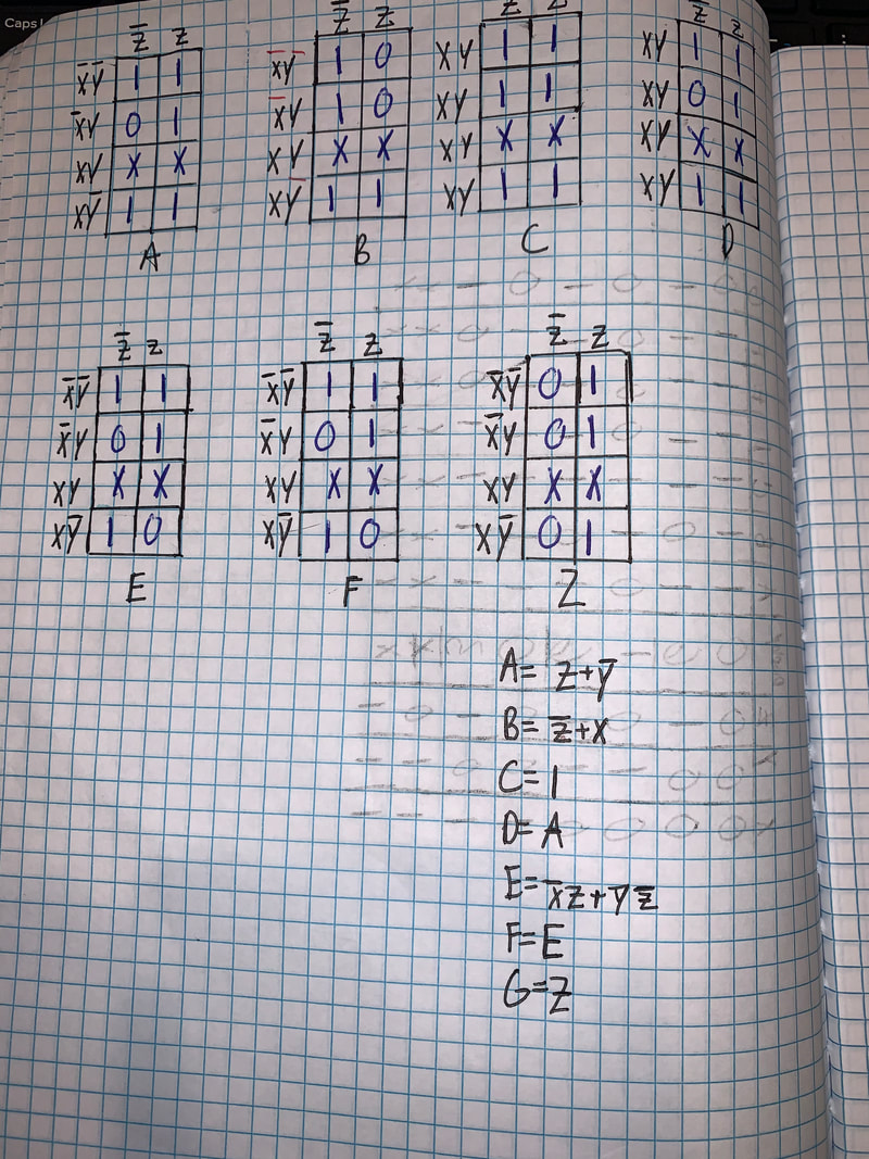
When K-mapping we started by creating small charts(k-maps) for each variable in our truth table, and labeling the sides X, and Y while the top was labeled Z. The charts were 4 by 2, with X'Y',X'Y,XY and XY' on the side and Z',Z on the top. After creating each chart needed then we would fill the chart with our display values starting from the top of our truth table working our way down to fill the chart from left to right and switching the 3rd and fourth terms. For example the order of the pairs would be 1st,2nd then 4th and 3rd. After filling each chart you would then go through and group the 1's and X's to create the most simplified logic expression. The final expressions are written in sum of product form making it easier to create our AOI circuits that would be later changed to NAND or NOR circuits.In total i had seven k-map, one for each variable in my common cathode.In the end i had two logic expressions that were the same as another, one that had an output of 1, and a logic expression with one variable due to the entire side of the chart canceling leaving only what was on the top. K-mapping is a lot more organized and easier to simplify the with boolean algebra.
MultiSim Implementation
The image below shows my circuit using the Multisim program.In this circuit there was a mix of an AOI, NAND and NOR circuit which are connected to resistors and the common cathode.
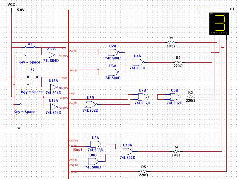
I created my circuit in bus form so that it would be easier to read and create on my breadboard.For my circuit i needed 3 inverter gates, 2 and gates, 1 or gate, 3 NAND gates and 3 NOR gates meaning in total i needed 6 chips.We used NAND and NOR gates because it helps decrease the amount gates that would be needed.But it may not always work for example the AOI circuit for "E" only uses 3 gates in total not including the inverters however the NOR circuit for "E" uses 8 gates in total in the un-simplified version. This is important because depending on the amount of chips that are used can either lower or increase the cost of materials for your circuit. A seven segment display works when a circuit is connected to each of the seven segments. There are to types of seven segment display common cathode and common anode. For our circuit we used a common cathode segment display.The difference between common cathode and anode is that for cathode we would connect it to ground and the segments that we want to appear would be connected to power while common anode is reversed. We used common cathode because the logic board we used works with a common cathode. The resistors in the circuit resist the flow of power that goes into the display so that it does not overheat or get destroyed.
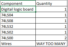
Bill of Materials
This describes the amount of specific IC chips that were used to create the circuit.
Date of birth circuit bill of materials
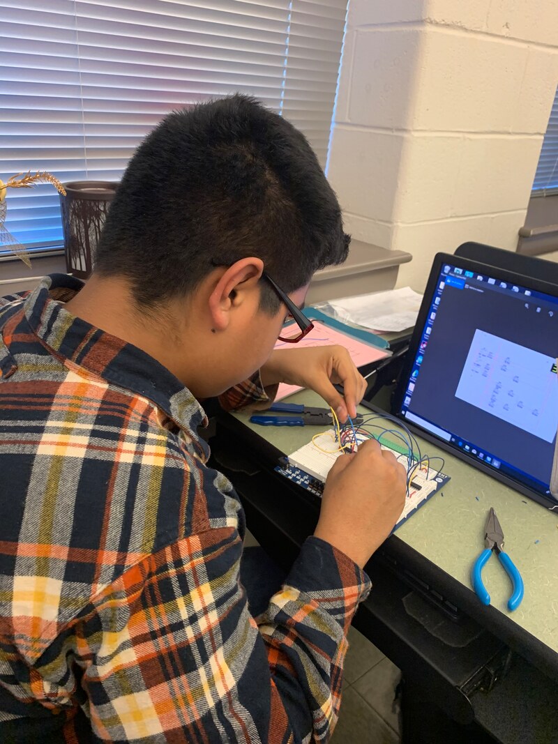
Bread-boarding
My second bread-boarding experience was very stressful. Because my multisim circuit was not correct it caused me to create a prototype that didn't work at all. This bread board was also very difficult to keep neat and not accidentally pull out wires when placing new ones. In my opinion i don't think color coordinating would've helped much with making it uncluttered, except for knowing what variable is what. Some other mistakes i made were forgetting to use a 74LSO8 chip for my circuit, and placing my chips right next to each other. Some skills i learned was that after wiring one of my minterms to check if it worked when it was supposed to in my circuit, instead of waiting to the very end to check my circuit and having to sift through all the wires to find the problem while i could be causing more problems with moving the wires. I also had to keep an eye on my NOR gates because they are reversed unlike the other chips. After much troubleshooting with each minterm, my circuit finally worked but one negative thing about my circuit is that i had to make sure all my chips were pressed down unless some of the display wouldn't show.
Conclusion
From this project i learned how difficult bread-boarding can be sometimes, but in the end it does create a satisfying feeling knowing that all the hard work payed off and it works. I also got a better understanding of how to bread board AOI, NAND and NOR circuits. Another important thing i learned about this project is that whenever your bread-boarding or creating a circuit you have to be patient with it and always triple check your work to make sure you made no mistakes. Something that i would do differently next time is that i would have space in between my chips so its not so close together and i would also color code so that finding my mistakes would be a little easier. There aren't many questions i have except why is the NOR chip reversed?
Extra credit
|
My AOI circuit was the easiest and most efficient to make only using 4 chips in total
|

|

